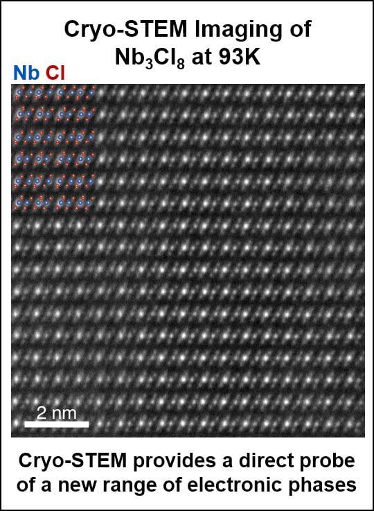
Being able to see and to measure down to a single atom helps us uncover some of the mysteries of science, technology and nature. Electron microscopy has enabled imaging of our natural word with exceptional detail. Today, the three-dimensional structure of biomolecules can be studied down to the atomic scale and single defects present in atomically thin materials can not only be identified but also spectroscopically probed. The developments that have enabled these successes in the life sciences and the physical sciences have been recognized by the 2017 Nobel Prize in Chemistry and the 2020 Kavli Prize in Nanoscience. Despite these breakthroughs in imaging there are entire classes of materials and devices that have not been able to be explored at the relevant microscopic length scales. New innovations—in hardware, in imaging methods and in data analytics—are needed to drive electron microscopy forward.
Our group focuses on opening new windows into the microscopic word by advancing cryogenic electron microscopy techniques to answer questions such as: How can we understand the complexities of quantum phases that emerge at low temperature? What limits the performance of energy devices—systems that often involve liquids, reactive species or soft-hard interfaces that cannot be studied with traditional electron microscopy techniques?
Atomic-resolution, picometer-precision cryogenic STEM imaging
 Mapping lattice displacements in crystals requires high-precision measurements of the atomic positions. At room temperature this has been demonstrated and applied on a number of systems. In all of these examples, multi-image registration is critical for high fidelity image reconstruction. Such registration is, however, challenging in cryo-STEM, where reduced mechanical stability due to LN2 cooling necessitates rapid acquisition and therefore results in low signal-to-noise ratios.
We have developed a registration approach optimized for low signal-to-noise STEM data. By registering all possible pairs of images and enforcing physical consistency between a surplus of measurements, we can identify and account for incorrect registrations due to unit-cell misalignments and produce high-quality image reconstructions. Using this technique, we have demonstrated <0.8 Å information transfer at cryogenic temperatures and thereby enabled high-precision measurements of low temperature phases.
Select publications
Atomic-resolution cryogenic scanning transmission electron microscopy for quantum materials | Elisabeth Bianco, et al., Accounts of Chemical Research 54, 3277 (2021)
Atomic-resolution cryo-STEM across continuously variable temperature | Berit H. Goodge, et al., Microsc. Microanal. 26, 439 (2020)
Direct Visualization of Trimerized States in 1T′−TaTe2 | Ismail El Baggari, et al., Phys. Rev. Lett. 125, 165302 (2020)
Nature and evolution of incommensurate charge order in manganites visualized with cryogenic scanning transmission electron microscopy | Ismail El Baggari, et al., Proc. Natl. Acad. Sci. 115, 1445-1450 (2018)
Image registration of low signal-to-noise cryo-STEM data | Benjamine H. Savitzky, et al., Ultramicroscopy 191, 56 (2018)
Enabling atomic-resolution chemical mapping at cryogenic temperatures
More efficient detectors hold great promise for atomic-resolution EELS mapping at cryogenic temperatures. In 2017, we installed a direct electron detector (DED) (Gatan K2 Summit) on our cryo-STEM. Unlike indirect, scintillator-based detectors, DEDs collect electron-hole pairs and, consequently, improve the detector quantum efficiency, the point spread function, and the signal-to-noise ratio. We have demonstrated that these improvements are especially critical for atomic-resolution EELS applications that require low-dose or rapid-acquisition such as when operating in cryogenic conditions. Even at a relatively short dwell time (2.5 msec/pixel), the signal-to-noise ratio of the spectra recorded using a DED camera remains high, allowing atomic-resolution elemental mapping near liquid nitrogen temperature. Elemental maps are, however, not sufficient. We are now working on further improvements to perform true atomic-resolution spectroscopic mapping at cryogenic temperature.
Beyond Liquid Nitrogen Cooling
Liquid nitrogen specimen cooling inside the STEM has provided access to a new range of quantum phases. Nevertheless, many more remain out of reach for atomic-resolution characterization. In the coming years, our goal is to extent atomic-resolution cryogenic STEM to lower temperatures in order to be able to probe electron, lattice, spin and orbital order of quantum materials. This will required significant advances in hardware, but will open a new window into the microscopic underpinnings of quantum phases.
