Atomically abrupt oxide interfaces

High-angle annular dark field images of a La0.7Sr0.3MnO3/SrTiO3 superlattice grown by pulsed laser deposition. The view is down the [100] zone axis of the SrTiO3 substrate. Right, a magnified view shows atomically sharp interfaces between the two materials.

Cryo-STEM mapping of solid-liquid interfaces in Li-metal batteries

Direct observation of the anode–electrolyte interface in a Li metal battery reveals two types of dendrite, one of which may contribute disproportionately to capacity fade.

Bending and breaking of stripes

In charge-ordered phases, broken translational symmetry emerges from couplings between charge, spin, lattice, or orbital degrees of freedom, giving rise to remarkable phenomena such as CMR and MIT. To understand the role of the lattice in charge-ordered states, we directly map picometer scale periodic lattice displacements at individual atomic columns in the room temperature charge-ordered manganite using aberration-corrected STEM.

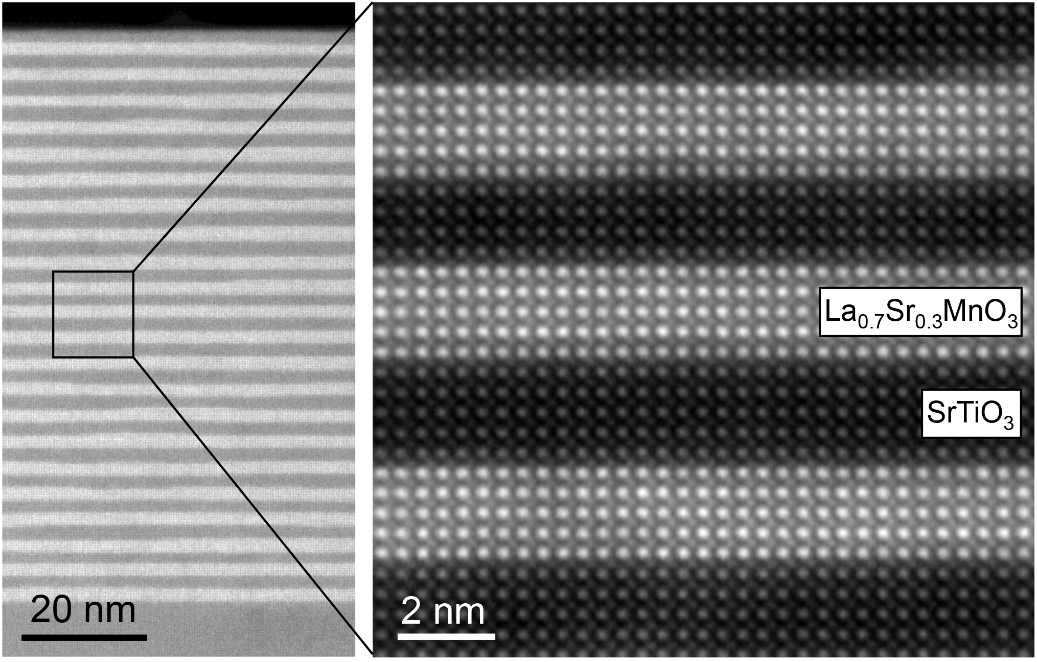
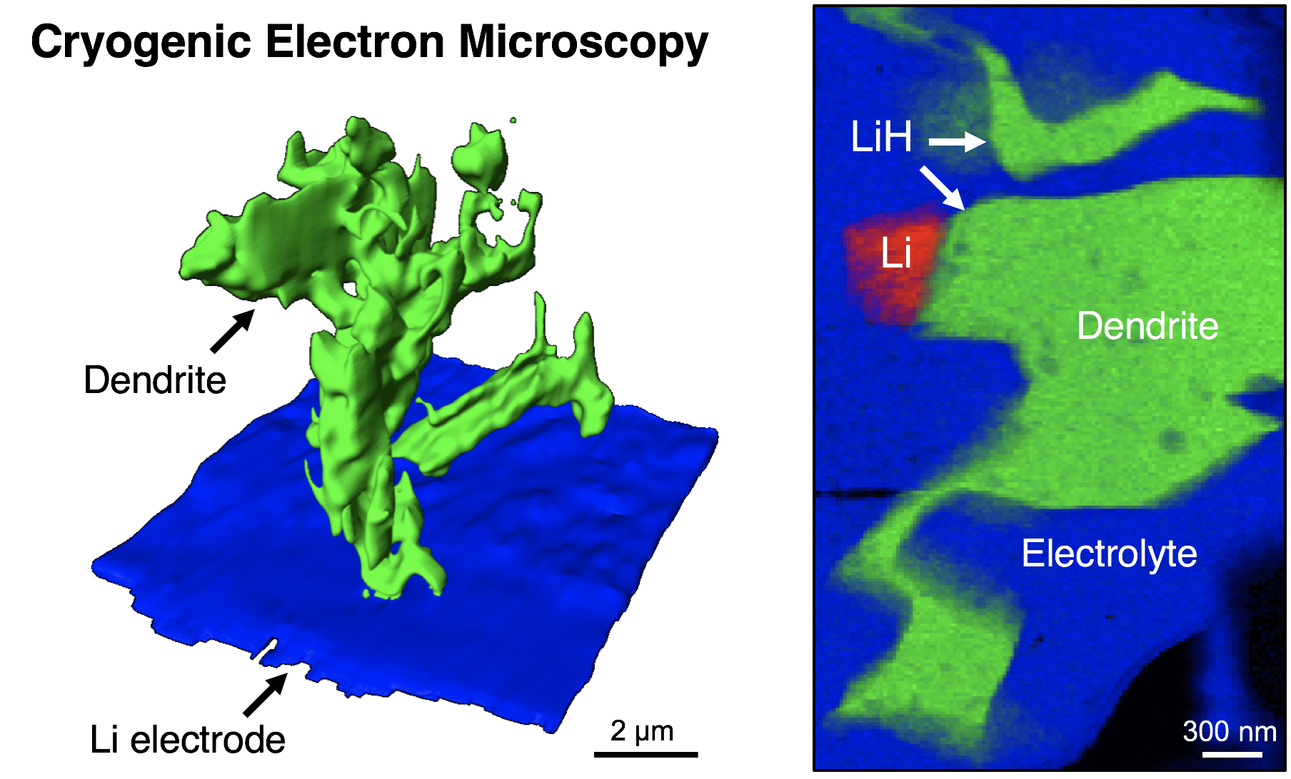
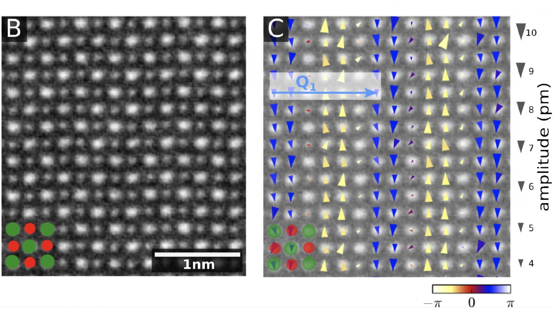
The Kourkoutis electron microscopy group develops and applies novel electron microscopy techniques to advance the fundamental understanding of materials and devices. Central to all of these efforts is the scanning transmission electron microscope (STEM), a tool that allows us to probe structural, chemical and electronic properties at the atomic scale.

Explore our Research Topics